Question to the Al..

Posts
40
Likes
118
Hello.
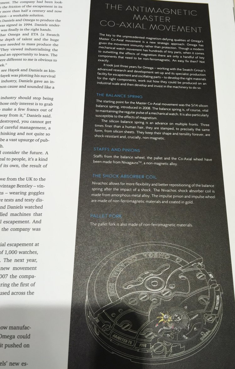
I just read from Omega Lifetime issue that the new Master co-axial movement has impulse wheel made of non-ferromagnetic material and coated in gold.
Now i wonder, how a thin layer of gold can resist wear and tear in a such place ?
 
Posts
27,352
Likes
69,745
Not familiar with whatever the Lifetime thing is - sounds like a magazine. If so, they don't give that sort of stuff to us lowly watchmakers...even though I spend more with them for parts than most people here do on watches each year...

Anyway, doing some translation, I suspect by impulse wheel that means co-axial wheel. If so, it may be gold coloured, but I doubt it's actually coated in Au. There are gold coloured parts used in various movements, and I don't think any of them are actual gold. Could be something like a TiN coating perhaps...if you could direct me to the article if it is on line, or provide a shot of it here if it is a magazine, I could dig into it further...

Cheers, Al
 
Posts
158
Likes
184
I think I found the article! It's an Omega magazine that they send out to customers
 
Posts
44
Likes
26
a6698ee0fecf12f59843470c968925b5.jpg
Hi,
I think I found what OP i referring to.
 
Posts
27,352
Likes
69,745
Well, it says what it says, but I am skeptical of the accuracy of marketing materials like this...for example they say the silicon balance springs are "stamped" which is a very poor descriptor of the technology used.

Nothing in the description of the co-axial wheel on the Omega Extranet indicates it is gold plated. To me that would be a very poor choice of materials based on some of the wear I see on these wheels...

Cheers, Al
 
Posts
44
Likes
26
the silicon balance springs are "stamped" which is a very poor descriptor of the technology used.

In the same magazine the process is described as follows: "The Si14 silicon balance spring is produced using an advanced manufacturing process called photolithography. A silicon wafer disc is coated with a nanometre thick layer of photosensitive resist. A metal coated mask - a super detailed stencil of the springs - is then matched with the silicon disc and is exposed to ultraviolet light. Unmasked parts of the photoresist, altered at the molecular level, can then be chemically washed away while another chemical agent, with the assistance of a blast of charged ions, etches into and removes the silicon around the resist. The resist is finally removed by another agent, revealing the perfectly formed springs."

Easy peasy 😀

Jens
 
Posts
29,513
Likes
35,471
Easy peasy 😀

Jens

Surprisingly enough it actually would be, especially for making something as basic as a balance spring rather than the purpose those particular manufacturing methods were originally design for 😉
 
Posts
27,352
Likes
69,745
In the same magazine the process is described as follows: "The Si14 silicon balance spring is produced using an advanced manufacturing process called photolithography. A silicon wafer disc is coated with a nanometre thick layer of photosensitive resist. A metal coated mask - a super detailed stencil of the springs - is then matched with the silicon disc and is exposed to ultraviolet light. Unmasked parts of the photoresist, altered at the molecular level, can then be chemically washed away while another chemical agent, with the assistance of a blast of charged ions, etches into and removes the silicon around the resist. The resist is finally removed by another agent, revealing the perfectly formed springs."

Easy peasy 😀

Jens

Yeah, like they said...stamped...::facepalm1::

There is actually a very specific process used, but I can't recall the acronym for it.
 
Posts
27,352
Likes
69,745
Surprisingly enough it actually would be, especially for making something as basic as a balance spring rather than the purpose those particular manufacturing methods were originally design for 😉

Well, yes and no. The spring itself is easy yes, as would the collet by itself and stud. Doing them all together as one piece, not so much. This is why the original iterations were assemblies made of more than one part, rather than the more advanced process used now that creates it all in one go...
 
Posts
287
Likes
473
In the same magazine the process is described as follows: "The Si14 silicon balance spring is produced using an advanced manufacturing process called photolithography. A silicon wafer disc is coated with a nanometre thick layer of photosensitive resist. A metal coated mask - a super detailed stencil of the springs - is then matched with the silicon disc and is exposed to ultraviolet light. Unmasked parts of the photoresist, altered at the molecular level, can then be chemically washed away while another chemical agent, with the assistance of a blast of charged ions, etches into and removes the silicon around the resist. The resist is finally removed by another agent, revealing the perfectly formed springs."
I know that sounds fancy, but that's how computer chips have been made for decades.

When I was in college, I used the process to make microfluidic devices for cell research. Even I can do it.

edit: here's a video explanation for something more complicated (ie multilayered) than the balance spring.

Edited: